
Securing the AIoT Ecosystem: Semiconductor Innovations in Device Management
Securing the AIoT Ecosystem explores how cutting‑edge semiconductors bring edge AI, energy efficiency, and hardware‑rooted security to large‑scale device management.
What makes this process possible isn’t just clever software. It’s the silicon underneath. Today’s semiconductors have evolved into computational powerhouses that were unimaginable just a decade ago. Engineers are now embedding specialized AI accelerators directly into microcontrollers, creating chips that can run complex neural networks while consuming minimal power. These are heterogeneous computing platforms that combine traditional processing with neuromorphic architectures designed to mimic the human brain’s information processing capabilities.
The numbers tell a compelling story. Industry analysts project that 75% of AIoT devices will rely on energy-efficient, purpose-built hardware by 2030. But behind these statistics lies a fundamental shift in how we think about computation itself. Rather than shuttling data back and forth to distant cloud servers, intelligence is moving to where it’s needed most, right at the source of data generation.
In this article, we’ll explore how semiconductor innovation is not only fueling AIoT’s expansion but also playing a pivotal role in securing the ecosystem through advanced device management at the edge.
The transition from centralized cloud processing to distributed intelligence at the edge represents an important shift in how computing is designed and deployed in the era of AIoT. This is not simply a matter of optimizing performance. It is a direct response to real-world constraints and demands: the need for ultra-low latency, bandwidth efficiency, enhanced data authority, and autonomous operation in disconnected or bandwidth-limited environments. In mission-critical domains such as autonomous vehicles, smart manufacturing, and real-time health monitoring, relying on cloud-based decision-making can introduce significant delays. In such contexts, even a fraction of a second matters. As these use cases multiply, the traditional cloud-centric architecture proves insufficient, pushing the industry to rethink the entire computational model.
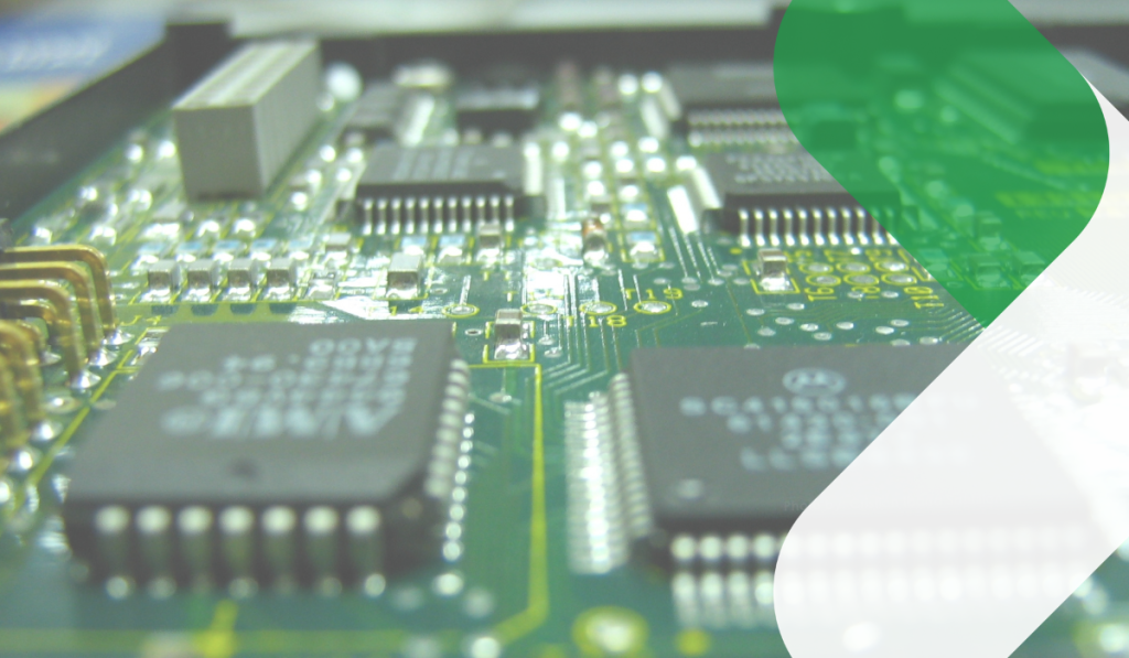
The semiconductor industry has risen to meet this challenge with some genuinely impressive engineering. Modern chip design is rapidly evolving to meet the requirements of edge AI, with a focus on energy efficiency, high computational density, and adaptability. Advanced process nodes, such as 5nm and 3nm technologies, enable the integration of billions of transistors into compact, low-power packages. These capabilities are especially critical for battery-operated IoT devices, which must run AI workloads locally without frequent cloud interaction. Today’s cutting-edge silicon not only supports localized inference and pattern recognition but also enables adaptive behavior in real-time, even within resource-constrained environments.
However, the semiconductor landscape is not only defined by technological breakthroughs. Economic forces and strategic considerations also shape it. The global semiconductor market is expected to expand by over $157 billion between 2025 and 2029, driven by significant growth in the increasing adoption of IoT devices across various domains, including industrial, automotive, and urban infrastructure. Each of these verticals comes with unique technical requirements: industrial IoT demands durable, long-lifecycle chips capable of withstanding extreme conditions. The automotive sector requires high-performance, safety-certified silicon to support driver assistance systems and autonomy, and smart city applications rely on semiconductors that can endure variable climates while powering expansive sensor networks.
Adding to these technical demands are broader concerns about supply chain stability and geopolitical dynamics. Recent chip shortages have exposed vulnerabilities in global manufacturing ecosystems, prompting a wave of investment in domestic fabrication capabilities and technology sovereignty initiatives across North America, Europe, and Asia.
IoT is experiencing a dramatic growth in scale, with projections indicating that over 75 billion devices will be connected to the internet by 2025. This remarkable growth is not just a matter of quantity. It fundamentally transforms the way we generate, transmit, and process data. From environmental sensors and smart meters to industrial machines and connected vehicles, each device continuously produces data streams that capture everything from physical conditions to user behaviors. These data streams must be processed either in real-time or near real-time to enable intelligent decisions, responsive systems, and predictive maintenance across diverse industries.
This level of data generation places unprecedented strain on conventional computing models. Centralized cloud architectures, while powerful, simply cannot accommodate the bandwidth requirements or meet the ultra-low latency demands of tens of billions of simultaneously active devices. As a result, we are witnessing a paradigm shift toward distributed computing, where intelligence is directly embedded into devices and localized edge infrastructure. In response to this need, the semiconductor industry is rapidly innovating to develop highly specialized chips that can handle dedicated tasks, such as sensor fusion, anomaly detection, and pattern recognition, directly on the device, thereby bypassing the delays and constraints of cloud-based processing.
The rapid expansion of the IoT landscape would not be possible without equally rapid innovation in semiconductor design. At the heart of this evolution are chips explicitly engineered for the unique challenges of IoT environments, where power efficiency, compact form factors, and cost-effectiveness are non-negotiable. Today’s low-power IoT processors utilize dynamic voltage and frequency scaling (DVFS), power gating, clock gating, and adaptive body biasing techniques, which have been shown to reduce energy consumption by up to 60%. This enables devices to operate for years on a single battery, even under complex workloads.
Mihai Petre, Technical Lead at rinf.tech, points that "embedded systems are specialized computers designed for a specific task, and they need to perform it well. However, this isn't always the case. Practical experience from past projects is crucial for designing solutions that effectively meet customer needs, balancing factors like production cost, features, and power consumption"
According to Mihai, "Since embedded systems are built for specific jobs, their hardware and software are often tightly coupled. This means that if a significant hardware design flaw occurs, software engineers must devise creative workarounds to ensure functionality. Therefore, embedded software engineers must be an integral part of the entire solution. They need to communicate closely with hardware engineers and actively participate in the schematic and layout design processes. In several projects, having a team member with even a basic understanding of analog design could significantly reduce software development time and costs. Furthermore, effectively leveraging the capabilities of modern CPUs (MCUs, MPUs) can often simplify the overall solution and reduce the Bill of Materials (BOM) due to their high degree of peripheral integration."
Moreover, optimizing processor instruction sets and execution pipelines for IoT-specific workloads reduces overhead and improves overall energy efficiency. These advancements are particularly crucial in sectors like industrial automation, agriculture, and healthcare, where devices often operate in remote or infrastructure-limited settings and must function reliably over long lifecycles with minimal maintenance.
A major breakthrough in enabling intelligent IoT devices has been the integration of AI capabilities directly into microcontrollers and system-on-chip (SoC) devices. Companies like Ceva are leading the charge with innovations such as the Ceva-NeuPro-Nano, an ultra-efficient neural processing unit (NPU) designed to bring Edge AI and TinyML capabilities to resource-constrained environments. These NPUs are purpose-built to execute machine learning inference workloads with minimal power draw, making it feasible to run AI models directly on the device itself.
By embedding AI acceleration within the same chip as the main processing unit, system complexity is dramatically reduced. There’s no need for a dedicated AI processor, which lowers both the cost and power consumption of the overall system while improving performance, reliability, and time-to-market for AIoT solutions.
Edge computing is rapidly redefining the way data is processed in the IoT landscape. Instead of sending raw data to the cloud for analysis, edge computing enables devices to process and interpret information at the source where it’s generated. This shift is more than a technical improvement. It’s a necessary evolution for time-sensitive applications that depend on instant reactions. In sectors such as autonomous mobility, industrial safety, and real-time medical diagnostics, decisions must be made in milliseconds or less. The traditional round-trip to the cloud introduces delays that these applications simply can’t afford. By enabling local decision-making, edge computing reduces latency and also conserves bandwidth, making systems more responsive, efficient, and scalable.
Another advantage lies in privacy and data security. By keeping sensitive data close to the source, within the device, or on local infrastructure, organizations can dramatically reduce the risks associated with data transmission and centralized storage.
The ability to process AI workloads at the edge has been made possible thanks to rapid advancements in semiconductor design. Companies like Arm are leading the way with purpose-built microcontrollers and neural processing units (NPUs) explicitly tailored for high-performance edge AI applications. Arm’s 2024 launch of the Ethos-U85 NPU, for example, marks a significant leap forward, delivering up to four times the performance improvement for real-time use cases such as factory automation, smart surveillance, and embedded vision systems. These processors are designed to execute neural network tasks efficiently while adhering to the strict power and thermal constraints of edge environments.
Neural processing units are particularly instrumental in bringing AI capabilities to edge devices without overloading them. Unlike general-purpose CPUs or even GPUs, NPUs are specifically architected to perform high-precision AI functions, such as convolution, pooling, and activation, with minimal power consumption.
As billions of devices connect to global networks, security becomes a defining concern for the Internet of Things. Ensuring the integrity, confidentiality, and authenticity of data and operations across this vast, distributed ecosystem requires security to be embedded not as an afterthought but as a foundational design principle, starting from the silicon level.
As Adrian Herea, Technical Lead at rinf.tech, emphasizes, "technology is generally employed to solve specific problems and enhance human lives. However, integrating technology into daily life necessitates accepting that potential benefits often come with associated risks. Depending on their application, E/E (Electrical/Electronic) systems can introduce hazards and various threats during operation. Despite the increasing complexity of embedded systems, ensuring predictability requires a development process that guarantees strict specialization of all integrated components, whether software or hardware. This specialization also positively impacts power efficiency."
From Adrian's perspective, "In any final system, the overall level of safety and security is determined by its weakest component (software or hardware) contributing to a specific functionality, as well as the weakest phase in its development or production. The inclusion of various accelerators, including AI accelerators, within an embedded system introduces a new layer of complexity, balanced by increased capabilities such as improved vision for autonomous vehicles. With the integration of AIoT, the complexity of the full system rises, opening new opportunities like automated factories and autonomous agriculture. To ensure an E/E system is safe and secure, especially when its development involves multiple contributors, it is mandatory for all parties to follow a unified development process blueprint for the entire system. This can be achieved by adhering to common industry-specific standards, which helps reduce the risk of hazards and security threats to a maximally acceptable level. Nevertheless, simply following standard guidelines is often insufficient to achieve a truly safe and secure system. Therefore, expertise in embedded development is crucial to mitigate risks in the final system, where hardware and software converge, preventing harm to individuals or unauthorized access to sensitive assets."
One of the most critical mechanisms in defending IoT devices against cyber threats is the secure boot process. At its core, secure boot ensures that only trusted, digitally signed firmware can be loaded and executed on a device. This protects against malicious code injection during startup, one of the most vulnerable moments in a device’s lifecycle. By validating firmware integrity before execution, secure boot establishes a chain of trust that supports the entire software stack, from the bootloader to the operating system and up to the application code.
Implementing secure boot in an IoT environment relies on cryptographic verification techniques anchored in hardware. These anchors, usually embedded in tamper-resistant hardware security modules (HSMs), store sensitive assets such as cryptographic keys and root certificates. During the boot sequence, each software component is checked for authenticity before execution, forming a verifiable path from immutable hardware roots to all operational layers.
Beyond secure boot, hardware security can be further strengthened by integrating Physical Unclonable Functions (PUFs), a novel and highly effective method of generating chip-level cryptographic identity. PUFs exploit natural manufacturing variations in silicon to create a unique physical fingerprint for each device. These unpredictable, unclonable characteristics are then used to derive encryption keys and identifiers without storing them in memory, reducing the risk of key extraction or duplication.
Among the most efficient PUF implementations for IoT is SRAM PUF technology, which leverages the inherent randomness of SRAM cell start-up behavior. It can be used to derive cryptographic keys on demand securely, eliminating the need for separate key storage and thereby minimizing the system’s attack surface. In resource-constrained environments, such as those found in wearables, sensors, or smart meters, PUFs offer lightweight yet powerful authentication mechanisms that enhance both security and efficiency.
While initial deployment is essential, long-term device security hinges on the ability to manage firmware updates securely. Yet, in the world of IoT, this is far from simple. Unlike traditional IT systems, IoT deployments often involve thousands, or even millions, of devices spread across various zones, operating in challenging environments, and connected through intermittent or low-bandwidth networks. Managing firmware updates for such a vast, heterogeneous fleet introduces a range of logistical and technical challenges.
Many IoT devices operate unattended, with limited memory, processing power, or battery life, making traditional update models unsuitable. Variability in hardware configurations, operating systems, and communication protocols further complicates the creation of a unified update strategy. More importantly, the risks associated with firmware tampering are significant: a compromised update can serve as an entry point for malware, backdoors, or data exfiltration, threatening not only individual devices but also entire networks or critical infrastructure systems.
To address these challenges, modern semiconductor architectures are embedding robust security features directly into the chip. These include secure storage for cryptographic assets and isolated execution environments designed to verify, authenticate, and apply firmware updates securely. For instance, firmware updates are often encrypted and digitally signed, ensuring that only verified, tamper-free code can be deployed. Additionally, anti-rollback protections are enforced to prevent attackers from installing outdated and potentially vulnerable firmware versions.
Some chipsets now feature dedicated security processors, separate from the main application processor, that handle cryptographic operations, manage secure boot processes, and validate firmware updates. These isolated cores prevent sensitive cryptographic material from being exposed to the rest of the system, creating a tamper-resistant environment for critical operations. Integrated Hardware Security Modules (HSMs) and root-of-trust architectures further enhance security by ensuring that the entire firmware update process, from validation to installation, is verifiably secure.
As the AIoT ecosystem continues to evolve, semiconductors will remain at the heart of its transformation. The coming decade will not simply be about incremental improvements in speed or efficiency. It will be defined by breakthroughs in materials science, chip architecture, and quantum-scale technologies that will unlock a new generation of intelligent, autonomous, and highly secure connected systems.
Tomorrow’s semiconductors are being shaped today in research labs around the world, where engineers and scientists are exploring new approaches to chip design far beyond the conventional boundaries of CMOS. Quantum tunneling, once a limitation, is now being engineered to support entirely new functionalities. Quantum dots, wells, and other quantum phenomena are being leveraged to develop true random number generators, ultra-secure key distribution systems, and energy-efficient computing blocks for highly specialized tasks.
Neuromorphic computing architectures are gaining traction as a way to mimic the human brain’s energy-efficient ability to process and respond to complex stimuli. These chips offer the promise of real-time learning and adaptive behavior, ideal for autonomous systems in unpredictable environments. Such innovations will push the boundaries of edge computing by dramatically reducing latency and power consumption while increasing processing efficiency.
As these emerging technologies mature, they will enable new classes of IoT devices, ones that are smaller, smarter, and more context-aware than ever before. Wearables that analyze biometric signals in real time, industrial sensors capable of anomaly detection without external input, and ultra-secure smart locks with embedded quantum security are just a few examples of what’s on the horizon.
We’re standing at a turning point. The semiconductor breakthroughs we’ve examined aren’t just gradual improvements. They’re fundamentally changing the rules of engagement for every industry touched by connected intelligence.
This transformation won’t wait for hesitant adopters. The companies already investing in next-generation silicon partnerships are building bridges that will be nearly impossible to cross later. They understand that in a world where every device makes autonomous decisions, the quality of those decisions depends entirely on the computational substrate beneath.
The technical demands are unforgiving. Tomorrow’s chips must juggle AI workloads that would have required server farms just five years ago, all while sipping power like a wristwatch and maintaining security standards. It’s a tall order that’s pushing engineers to explore exotic territories, neuromorphic architectures that mimic brain function, quantum effects that defy classical logic, and materials that barely existed in laboratories a decade ago.
The window for strategic positioning is narrowing fast. Organizations that treat semiconductor selection as an afterthought will find themselves building castles on quicksand, while those investing early in the right hardware foundations will unlock applications that seemed like science fiction just yesterday.
At rinf.tech, we’ve seen firsthand how the right software-hardware partnership can accelerate a company from concept to market leadership. We help bridge that critical gap where cutting-edge silicon meets real-world applications, turning semiconductor potential into a competitive reality.
Let’s talk.
Securing the AIoT Ecosystem explores how cutting‑edge semiconductors bring edge AI, energy efficiency, and hardware‑rooted security to large‑scale device management.
Voice recognition technology is revolutionizing industries, from automotive and retail to fintech and healthcare, by enhancing user experience and operational efficiency. However, as these systems become more integrated into our daily lives, robust security measures are essential to protect sensitive voice data from emerging threats like spoofing and unauthorized access.
Join rinf.tech at Embedded World 2025 to explore a new era in embedded innovation. At Booth 5-381 in Hall 5, discover our advanced LiDAR-Based Workplace Safety Solution—a system designed to enhance safety through dynamic, software-defined zones, real-time alerts, and intelligent operational insights. Learn how this versatile solution can be applied to diverse environments, from construction sites to production floors, ensuring a proactive approach to hazard detection and operational efficiency.
Copyright © 2023 rinf.tech. All Rights Reserved.
Terms & Conditions. Cookie Policy. Privacy Policy.
Politica Avertizari de Integritate (RO)